• New
    DE1-SoC Development Kit  (TERASIC) TA-P0159
    DE1-SoC Development Kit  (TERASIC) TA-P0159
    DE1-SoC Development Kit  (TERASIC) TA-P0159

    DE1-SoC Development Kit (TERASIC) TA-P0159

    TA-P0159
    €490.80

    409.00 € tax excl.

    DE1-SoC Development Kit  (TERASIC) TA-P0159

    Quantity :
    OUT OF STOCK

    DE1-SoC Development Kit  (TERASIC) TA-P0159

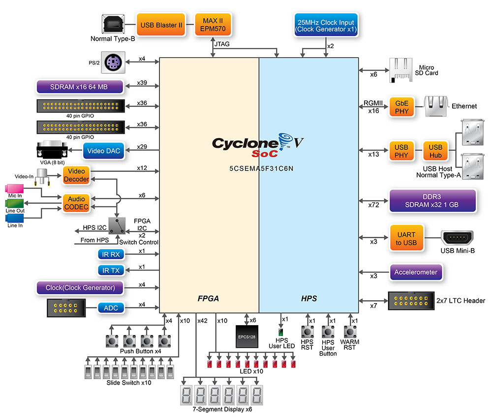
    The DE1-SoC Development Kit presents a robust hardware design platform built around the Altera System-on-Chip (SoC) FPGA, which combines the latest dual-core Cortex-A9 embedded cores with industry-leading programmable logic for ultimate design flexibility. Users can now leverage the power of tremendous re-configurability paired with a high-performance, low-power processor system. Altera’s SoC integrates an ARM-based hard processor system (HPS) consisting of processor, peripherals and memory interfaces tied seamlessly with the FPGA fabric using a high-bandwidth interconnect backbone. The DE1-SoC development board includes hardware such as high-speed DDR3 memory, video and audio capabilities, Ethernet networking, and much more.
    The DE1-SOC Development Kit contains all components needed to use the board in conjunction with a computer that runs the Microsoft Windows XP or later ( 64-bit OS and Quartus II 64-bit are required to compile projects for DE1-SoC  ). 
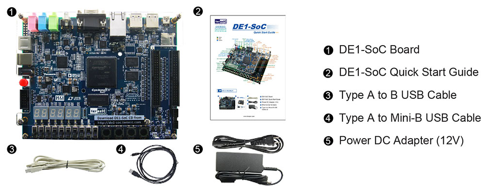
    FPGA Device

    • Cyclone V SoC 5CSEMA5F31C6 Device
    • Dual-core ARM Cortex-A9 (HPS)
    • 85K Programmable Logic Elements
    • 4,450 Kbits embedded memory
    • 6 Fractional PLLs
    • 2 Hard Memory Controllers

    Configuration and Debug

    • Serial Configuration device – EPCS128 on FPGA
    • On-Board USB Blaster II (Normal type B USB connector)

    Memory Device

    • 64MB (32Mx16) SDRAM on FPGA
    • 1GB (2x256Mx16) DDR3 SDRAM on HPS
    • Micro SD Card Socket on HPS

    Communication

    • Two USB 2.0 Host Ports (ULPI interface with USB type A connector) on HPS
    • UART to USB (USB Mini B connector)
    • 10/100/1000 Ethernet
    • PS/2 mouse/keyboard
    • IR Emitter/Receiver

    Connectors

    • Two 40-pin Expansion Headers (voltage levels: 3.3V)
    • One 10-pin ADC Input Header
    • One LTC connector (One Serial Peripheral Interface (SPI) Master ,one I2C and one GPIO interface )

    Display

    • 24-bit VGA DAC

    Audio

    • 24-bit CODEC, Line-in, line-out, and microphone-in jacks

    Video Input

    • TV Decoder (NTSC/PAL/SECAM) and TV-in connector

    ADC

    • sample rate: 500 KSPS
    • Channel number: 8
    • Resolution: 12 bits
    • Analog input range : 0 ~ 4.096 V

    Switches, Buttons and Indicators

    • 4 User Keys (FPGA x4)
    • 10 User switches (FPGA x10)
    • 11 User LEDs (FPGA x10 ; HPS x 1)
    • 2 HPS Reset Buttons (HPS_RST_n and HPS_WARM_RST_n)
    • Six 7-segment displays

    Sensors

    • G-Sensor on HPS

    Power

    • 12V DC input

    Block Diagram of the DE1-SOC Board

    image_77_thumb.jpg

    Kit Contents

    • DE1-SoC Board
    • DE1-SoC Quick Start Guide
    • Type A to B USB Cable
    • Type A to Mini-B USB Cable
    • Power DC Adapter (12V)

    image_72_thumb.jpg

    Terasic
    TA-P0159

    Specific References

    DE1-SoC Development Kit (TERASIC) TA-P0159

    €490.80

    409.00 € tax excl.